Pyra news partially stale from the dragon's mouth


For wavers, I assume you mean wafers, a term that usually applies to the thing inside modern integrated circuits, but I guess you're using it to describe the stacking of the multilayer boards - the bare PCBs. For some reason, CC with the pandora made all of the PCBs first then populated them, much later it turned out. I don't believe GC work like that, everything remains as data until it's ready to go then pcb etching and lamination happens, via's are punched, and then it goes straight through to population. I guess delays between stages might need to be managed, as glue takes time to dry, and washing off the etching fluid will need to be absolutely dry before lamination and gluing up, and it might not stay under the control of the machines all through those stages, it might well go into a bin and then be fed into the next machine, or it might be more like the 'inside the factory' shows I've watched where they have big spiral stacks for drying stuff out, and big long machines for baking, which the cakes and what have you travel through, which'd be more like for melting the solder paste in our factory. Sometimes doughs and things are made in a separate part and then wheeled through, but once everything is fed through to the production line nothing stops moving until it's being wrapped and loaded onto the van.
 
This is why i live mostly for myself, i dotnt friends, so comunication isnt something i make most of the time..
Shure, i have to deal whit customers, but this isnt that divicult..
I think he meant that mostly as a joke, as he implies, that he, as everyone around here, does not understand everything and that you by his idea should not write "I don't understand" but "We don't understand" :)
 
if you do not protect the pcb pads (where the components are soldered onto) because you do not expect long storage they will oxidize (rust) which makes machine soldering harder and failure rate goes up a lot

for commercial production failure rate is a real profitability killer

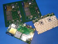
btw. inhouse pcb production is nuts ... these are 4 layer boards, imagine 16 layes or more :
 
That production board looks nice.
How much layers is the non-CPU board?
 

Attachments

  • twitter.jpeg
    twitter.jpeg
    333.5 KB · Views: 253
That production board looks nice.
How much layers is the non-CPU board?
Looking at my prototype from 2016, I can find nothing on it to indicate it's more than a 2 layer board. I can find no flood fill ground plane for example, other than parts visible on the underside of the board, and have as yet found no vias that don't go all the way through the board (although being under the white paint on the topside can sometimes be hard to spot).
 
For wavers, I assume you mean wafers, a term that usually applies to the thing inside modern integrated circuits, but I guess you're using it to describe the stacking of the multilayer boards - the bare PCBs. For some reason, CC with the pandora made all of the PCBs first then populated them, much later it turned out. I don't believe GC work like that, everything remains as data until it's ready to go then pcb etching and lamination happens, via's are punched, and then it goes straight through to population. I guess delays between stages might need to be managed, as glue takes time to dry, and washing off the etching fluid will need to be absolutely dry before lamination and gluing up, and it might not stay under the control of the machines all through those stages, it might well go into a bin and then be fed into the next machine, or it might be more like the 'inside the factory' shows I've watched where they have big spiral stacks for drying stuff out, and big long machines for baking, which the cakes and what have you travel through, which'd be more like for melting the solder paste in our factory. Sometimes doughs and things are made in a separate part and then wheeled through, but once everything is fed through to the production line nothing stops moving until it's being wrapped and loaded onto the van.
This is completely wrong, it doesn't work like that. The boards are produced and vacuum packed to prevent moisture ingress. Inside the pack is usually a card to show if the boards have been exposed to moisture. If the cards have been triggered the boards are 'baked' at a low temperature to remove the moisture, if this isn't done then they can delaminate when they go through the reflow oven, if this happens it can be very expensive as the board would be populated with expensive components at this stage.
 
So do the „Cards“ for the Pyra already sitting in Global Components?
And how good went the Testrun of the Boards?


Whit best regards, Matthias
 
The moisture cards usually have three/four circles on them, the circles are blue if not exposed to moisture and turn pink if moisture is present. The bare boards are usually unpacked just before applying bar code labels and screen printing.

These are typical cards:


These are used with MSD's (moisture sensitive devices) as well.
 
Last edited:
Looking at my prototype from 2016, I can find nothing on it to indicate it's more than a 2 layer board. I can find no flood fill ground plane for example, other than parts visible on the underside of the board, and have as yet found no vias that don't go all the way through the board (although being under the white paint on the topside can sometimes be hard to spot).
It's not unusual to also have multilayer boards with all via's going all the way through, it's cheaper to produce that way.
 
Back
Top