Global Chip Shortage Threatens Production of Laptops, Smartphones and More


There's been an opinion piece on el reg, which posits with apparently some evidence that china's new 7nm technology isn't all it's cracked up to be.
As also mentioned in the article, Chinese companies don't always perform the trick to actually scale. It can be to get funded or as a result of funding. The resulting production process isn't under 'control', so it doesn't scale and can't be really be put into practice outside of a laboratory. In case of SMIC they appear to have mastered the trick for this one chip. Doing it for any chip is a more difficult trick to perform. If it was so easy Samsung, which did 8nm on DUV, would have used it on 7nm also. But TSMC, Intel and Samsung all switched to EUV for this 7nm or smaller. So still a very great achievement on DUV, it's probably a one-trick pony that doesn't go any further (production scaling or sub-7nm).

If you think 7nm on DUV is much cheaper, because EUV is so expensive, it might not be.
- High-end DUV equipment reaches EUV costs.
- You need multiple reticle masks (the production step pattern for the wafer) and these costs a lot of money to produce.
- All the additional production steps cost time, money and drastically increase the chance of an error causing you workings chips to be lower. A chip that doesn't work doesn't make you money.
- All additional steps can be so costly in time the production takes way longer (instead of 2 months it's more like 6 months), also increasing the chance of having an outage / maintenance-routine during production (which increases the changes of production issues).
Most of these things are addressed by using EUV. EUV does require a completely new way of working, new factory and new equipment (which is very very expensive). So the initial investment is higher, but the result will be faster and better production. As EUV isn't available in China using DUV is their only option though.
 
As we were talking about smaller nm chips, these also get more sensitive to the following fenomena:
 
CNBC has some more footage and insights on the situation. Featuring some exclusive footage of ASML and TSMC. While TSMC's cleanroom footage is mostly dirt shoveling though.


Some corrections:
* ASML isn't an abbreviation (anymore), it's just a brand name now.
* DUV isn't only used for cheap low-end processors as mentioned. Also high-end chips use DUV (193nm wavelength) next to EUV (13.5nm), while lower-end might only use DUV. Because EUV is too costly to use exclusively and isn't as fast (165 wafers per hour) as some DUV systems (~300 wafers per hour). So you either use DUV systems only, or add EUV to the mix for specific parts of the process that requires it.
* It's mentioned TSMC has 5nm currently, while time moves on from when the video was made (same as this comment will age) TSMC already produces chips on 4nm (iPhone 14 and Qualcomm uses them), and TSMC is working on 3nm (release planned in 2023) and 2nm (planned for 2025) already.
* It's mention it was not logical Intel was failing so slowly with it's 10nm process, but I don't agree. Their process to shink worked for many years and this one kept feeling close and doable (but it wasn't). Which caused them to try out a lot of new strategies to make it work and those had somewhat of a limit success. Also EUV was so new at this time it didn't make sense to switch everything already, and EUV still required research and development to get working in the first place. SMIC got 7nm working also, just like Intel, so it's not impossible to do but just not ideal. If EUV was like it is today the situation indeed would not have made sense, Intel would have switched to EUV already for sure.
 
As also mentioned in the article, Chinese companies don't always perform the trick to actually scale. It can be to get funded or as a result of funding. The resulting production process isn't under 'control', so it doesn't scale and can't be really be put into practice outside of a laboratory. In case of SMIC they appear to have mastered the trick for this one chip. Doing it for any chip is a more difficult trick to perform. If it was so easy Samsung, which did 8nm on DUV, would have used it on 7nm also. But TSMC, Intel and Samsung all switched to EUV for this 7nm or smaller. So still a very great achievement on DUV, it's probably a one-trick pony that doesn't go any further (production scaling or sub-7nm).

If you think 7nm on DUV is much cheaper, because EUV is so expensive, it might not be.
- High-end DUV equipment reaches EUV costs.
- You need multiple reticle masks (the production step pattern for the wafer) and these costs a lot of money to produce.
- All the additional production steps cost time, money and drastically increase the chance of an error causing you workings chips to be lower. A chip that doesn't work doesn't make you money.
- All additional steps can be so costly in time the production takes way longer (instead of 2 months it's more like 6 months), also increasing the chance of having an outage / maintenance-routine during production (which increases the changes of production issues).
Most of these things are addressed by using EUV. EUV does require a completely new way of working, new factory and new equipment (which is very very expensive). So the initial investment is higher, but the result will be faster and better production. As EUV isn't available in China using DUV is their only option though.
Correction: TSMC N7 is still using (self-aligned) quadruple-patterning, only N7+ is using EUV. Meaning that also TSMC has these risks, hence they replaced 4 of these layers with EUV for N7+.
As TSMC used new design rules (a chips feature constraints derived from the limits of a specific fabrication process) for N7+ companies were hesitant to switch from N7 to N7+, so TSMC designed N6 to use the same design rules as N7. N6 replaces 5 layers with EUV.
 
Someone was so friendly to invite me to have a look in the joint lab from imec and ASML in Veldhoven (Netherlands). As to ASML policy it's no allowed to take pictures on their premise, so I'll try to convey the visit with some pictures I found online.
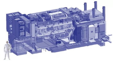
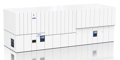
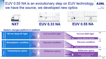
The lab contains all kinds of equipment including the latest-greatest High-NA system the EXE:5000. This system is still being assembled so it wasn't looking like the fancy images with outside covers on them, but it's actually nice to see the insides. It looks almost like one big sports engine. Obviously you'll need to suit up in a bunny suit to enter the cleanroom. The was a separate metrology room with some tooling to do metrology (measurements). The EXE:5000 is planned to be released in 2025 if I'm correct, and I think the first one is going to Intel.

How the system looks like when fully assembled (it's impressively big with fancy CNC manufactured shiny looking metal parts):
assembled.jpg
With covers on it would look something like this:
covers.jpg

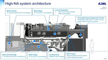
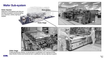
It appears there are actually slides online including ones showing some actual photos:
High-NA-system-architecture.jpg
shiny_metal_parts.jpg
EUV.png
 
Intel committed to start new factories in Europe and the most expensive one, a chip manufacturing plant (Fab 29), will be in Germany (Magdeburg, Saxony-Anhalt):
Germany and Intel Corp. sealed an agreement for the US company to receive an enlarged subsidy package worth about €10 billion ($10.9 billion) for a semiconductor facility in the former communist east, according to people familiar with the deal. Intel confirmed the accord Monday without providing a specific amount for the financial aid. It said it plans to invest around €30 billion in the “leading-edge wafer fabrication site” in Magdeburg, which Chancellor Olaf Scholz said represents “the single largest foreign direct investment in German history.”
Source: https://www.bloomberg.com/news/arti...ree-subsidies-for-chip-plant-worth-10-billion
Obviously I wouldn't mind to visit when it's finished, but first have them complete construction before I'll be opportunistically requesting a tour.

Intel will also build a packaging and testing facility in Poland. Since chiplets and wafer-bonding the packaging process can be very challenging.
More information on packaging and testing can be found here: https://news.skhynix.com/semiconduc...pisode-1-understanding-semiconductor-testing/

Intel would also create an R&D facility in France and potentially a new packaging facility in Italy. Intel already had a chip manufacturing facility in Ireland (Fab 24 and 34).
Next to Europe Intel might expand their facilities in Israel.
 
Back
Top