You are using an out of date browser. It may not display this or other websites correctly.
You should upgrade or use an alternative browser.
You should upgrade or use an alternative browser.
We've started to order things!
- Thread starter EvilDragon
- Start date
ClockworkCoder
Chaotic Neutral
Worst case, I'll just stick a dongle in it.Slightly worrying, no? The WiFi in the Pandora (or at least my Pandora) is awful
pmprog
DNF (Did Not Finish)
- Joined
- Apr 25, 2011
- Messages
- 4,150
Well, I do on my Pandora, but I was hoping to not have to do that with the Pyra, because I shouldn't have toWorst case, I'll just stick a dongle in it.
Stainy
Advanced Member
Is "almost done" a running gag?
That 'almost' doesn`t sound helpful ?
Kippykip
BFG 9000
It'll be just like the "Wheel of Monotony"That 'almost' doesn`t sound helpful ?
Mr_Loon
Can't Remember
- Joined
- Aug 30, 2010
- Messages
- 2,334
Great news ED.
Does the prototype you've produced have 4GB of Ram?
If yes then is that the first prototype with 4GB of Ram?
Do you still intend to mass produce the 2GB version?
If yes then could you do some benchmarks showing the impact on battery life & performance (compared to using the Nand for swap) for the 2GB & 4GB versions.
zmatt
Active Member
I propose we call this prototype "Patient Zero" or something sickly sounding and try to keep track of the number of prototypes and their stories from here on in. Do they get serial numbers? I'm sure one day I'll want to look back on these early devices. Can there be a wiki page?
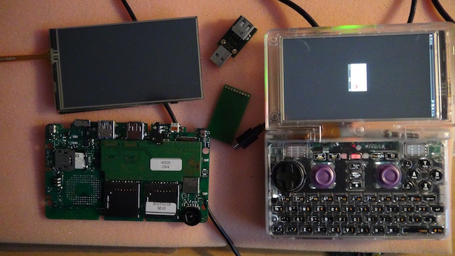
For your documentation collection:

Does the prototype you've produced have 4GB of Ram?
It should yes. One reason I've wired up the JTAG setup above is since it makes it easy to fiddle with memory config:

levi
Still fresh, damnit!
Well, that should be the situation give or take for the prototype boards, but retail boards should use that as a baseline and start from there.Slightly worrying, no? The WiFi in the Pandora (or at least my Pandora) is awful
rSl
tealifted
- Joined
- Nov 19, 2005
- Messages
- 1,141
Well, I do on my Pandora, but I was hoping to not have to do that with the Pyra, because I shouldn't have to
i also had bad wifi speeds with my 1ghz rebirth and used an external nano usb-dongle. then i changed my wlan-router, now using openwrt and did a fullflash with latest supersaxxon on the pandy.
i tried the onboard wifi again, and now it's completely ok! :-O so i don't have to use the external dongle any more which is great and should save some power not using the usb port.
sadly the pandora onboard wifi uses a lot of power too. here is hope that the wifi-chip of the pyra consumes way less power.
directive0
Very Active Member
For your documentation collection:
Thank you for your service Pyra-Typer.
hns
Well-Known Member
For extending the documentation...


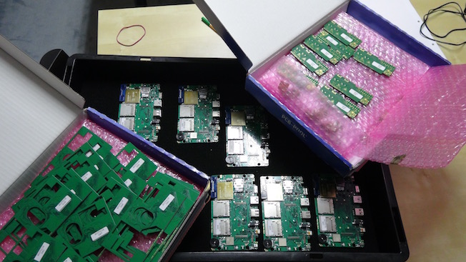
Now we have built both variants. I.e. ca. 50% of the CPU boards in the box in the upper right of the 2nd picture are with 2GB and the others with 4GB (can be identified by serial numbers). And the boards in the left picture are one with 2GB and one with 4GB.
zmatt has got a 4GB CPU board (which already runs with using only 2GB) since he has the best equipment (JTAG tools) and experience for making 4GB work. Now he is working to fix u-boot and kernel for 4GB (it needs the LPAE mechanism to allow for more than 2GB addressable memory).
Yes, the PCBs have serial numbers but not the assembled devices. And it is really difficult to define which one is the first one (there had already been approx. 10 before these ones in the last couple of months):I propose we call this prototype "Patient Zero" or something sickly sounding and try to keep track of the number of prototypes and their stories from here on in. Do they get serial numbers? I'm sure one day I'll want to look back on these early devices. Can there be a wiki page?
There had been one CPU board modded to have 3GB of RAM last summer. But we were lacking software to run it with more than 2GB.Great news ED.
Does the prototype you've produced have 4GB of Ram?
If yes then is that the first prototype with 4GB of Ram?
Now we have built both variants. I.e. ca. 50% of the CPU boards in the box in the upper right of the 2nd picture are with 2GB and the others with 4GB (can be identified by serial numbers). And the boards in the left picture are one with 2GB and one with 4GB.
zmatt has got a 4GB CPU board (which already runs with using only 2GB) since he has the best equipment (JTAG tools) and experience for making 4GB work. Now he is working to fix u-boot and kernel for 4GB (it needs the LPAE mechanism to allow for more than 2GB addressable memory).
rygD
Nihilistic Mystic
Maybe Almost Done should be the new Two Months. I would rather wait than have even more problems when I get the thing.Is "almost done" a running gag?
hns
Well-Known Member
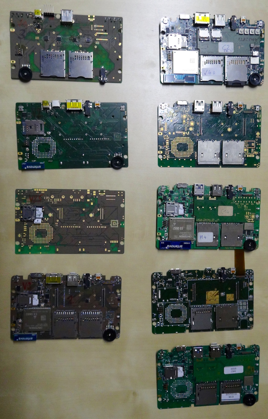
And here is one more picture for the historicans.
The evolution of all prototype generations of the PCBs in one picture...
V1 ............ V4
V2 ............ V4.5
V2.5 ......... V5
V3 ............ V5.1
................. V5.1.3
V1 was a first prototype to test the magnetic Nubs and get a general idea how it could look like
V2 got new shoulder buttons, s second USB port and the idea for a 3G/4G version and moved the potentiometer and connectors around
V2.5 got the idea for a replaceable CPU board (hence space for some - too small - B2B connectors)
V3 was the first one which worked with an adapter to the OMAP5432EVM and aligned connectors etc. with the plastics case design
V4 was the first one to work with a real CPU board
V4.5 got different SD slots and the eSATA connector was replaced by an USB3 socket
V5 changed the WLAN/Bluetooth module (the originally chosen one is no longer available) and became the first handful of prototypes shown e.g. last year at Gamescom
V5.1 tested a new µUSB3 connector and again a different SD slot
V5.1.3 is the latest production run with redesigned CPU boards (you can see a cut-out for the WLAN module)
V5.2 (no picture) is in the works resp. ordered - it will look like V5.1.3 and have only minor changes (e.g. CPU-Board and Antenna optimization)
PS: the backside is not that interesting - it shows the keyboard maeanders right from the beginning.
rygD
Nihilistic Mystic
Mmmm, purple nubs! 
ptitSeb
Serial Porter
levi
Still fresh, damnit!
@hns nice - that corresponds to out pre-preorder bonus bare pcbs declaring themselves as v5 boards.
Out of interest, what does the ~10mm square silver chip above the volume wheel (and with a CPU board cutout since v5.1-ish) do? I can't read the labelling from your image, and there doesn't seem to be a corresponding part on the Pandora boards, so I guess it's not the DAC.
And for completness, when did the keyboard reflector in white come in on the other side? And was the wonky chip always wonky?
directive0
Very Active Member
I propose we call them nurples.Mmmm, purple nubs!

