Hardware. Nubs and PCB pinout.


Gausen

Member
Joined
Dec 14, 2011
Messages
357
Age
46
Location
Buenos Aires, Argentina.
I didn't know where to put this question, I finally decided to use the support forum. Please move this thread as you see fit.

I was reading the wiki and couldn't find any info on nubs pinout. Does anyone knows how those six pads (question marker on the image) precisely relate to the nub pads?

Thanks in advance!
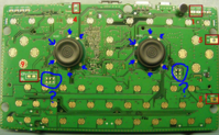
pcb.png
 
Thank you comrade! You have been most helpful.

Is this new? I've just downloaded this document (v100) this morning. In fact the attached image comes from that document.
 
According to the schematic on the last page of that hacker's guide, the nubs are on an I2C bus along with the battery gauge. Now, I don't know what the pinout on that pad is (assuming it's connected to each nub, which seems likely - but it'll be on the i2c bus so you'll probably see signals from all over). Using a multimeter it should be easy to determine which pads are VCC and which are GND, hopefully leaving two connectors, one of which will be clock, the other being data.

If you can build something that listened to i2c you can try wiring up those either way round till you find which way round works - I can't see that blowing anything up. Alternatively, if you have access to an oscilloscope, it should be easy to differentiate between clock against GND and data against GND.

If you do go to that effort, please let us know your findings. It'd be good to know a little more about how the magic nubs work, for out-of-lifetime hacking reasons.
 
Back
Top