skeezix
Internal Development
I've waffled on that very point many times; if you read the whole thread, I'm sure you'd see a pattern of indecision.. one big board! a separate gpu board, cpu board, power board, I/O board! No, how about a power and amp board, and cpu+gpu board! ... etc  Theres convenience vs cost vs placement advantage and such as well.
The sweet spot for pcbs these days is still 4"-square or less (10cm and less to a side); so, I've often liked the idea of a stack of 2 4"-square boards. I've even gone so far as to do a buss up one side, so that 2 or 3 or 4 boards could sandwhich together like that.. a cpu board, a gpu board, a power/audio board, an expansion/cart board on top. Think of the madness! I went once to the extreme, wher eyou could even stack multiple cpu boards ... and even so far as a crazy bus, where you could put like 32 cpu boards together for some crazy fun....
The trick of course is that microcontrollers, with the pincounts I need (100+), are pretty 'big' (their footprint, plkus the necessary space around them for the routed paths), so putting two of them on the same 4" surface is hard. But as they're smt, there _is_ the possibility of doing one on each side, but I find I need those vias and both sides to do the horrid routing. This of course is why modern pcbs are 4+ layers thick, so you can jam things in good and route all around no problem.
So, hence why I've settled on 6"x4" .. a little pricier, but at least its got the space to put the two chips on there, and also enough for a bunch of support stuff.
But yes, I could do a r4 with various combinations..
- a base 6"x4" board with most of the good stuff
- a shield that goes on, for all the jacks and breakout
--> but designed for this purpose
ie: group all the headers together in some central location, or convenient location (elevator shaft like).
Making r3 was _Really_ tough routing, because its a metric hellpile of traces; also, the chip pinouts are really bizarre.. like, you'd think they'd be in bamks of 8, like on 8bit chips like the atmel avrs .. so GPIO "bank A" would be A0-A7, right? But on these high pincount chips, they're will nilly, 100 or 144 pins all in a big random mess more or less. Seems to me like they lay out the internal mess and when they add the physical pins on, its 'best they can do, without much of a fight/cost'; real boards are BGA surface mount and auto-routed by million dollar software so who cares right? But us hobbyists agonizing ove cost and every trace, it hurts like hell
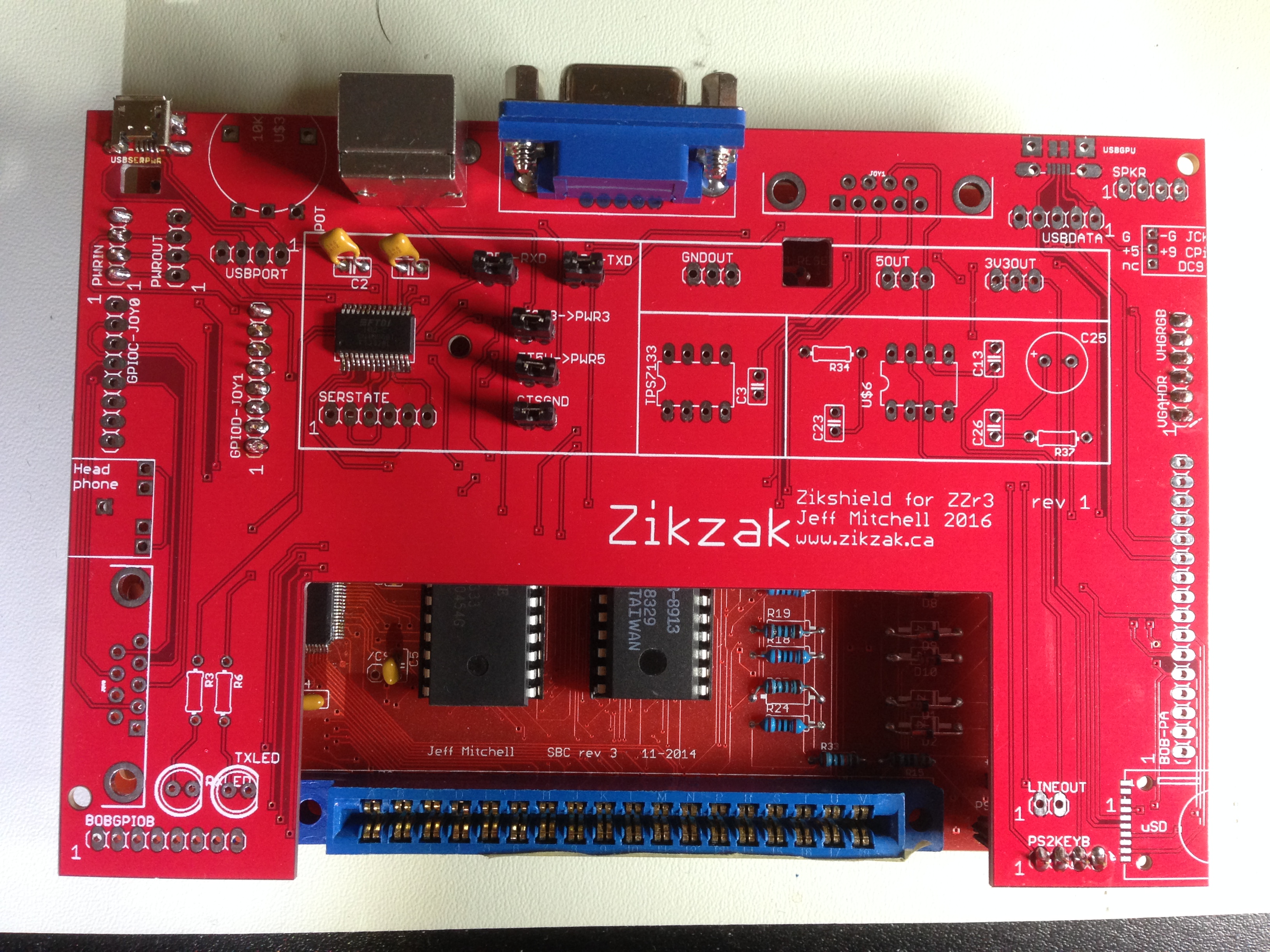
And as noted, making the eagle cad library for these little jacks and parts is fiddly work; so making this shield for r3 is really just a way to move forward 'path of least resistance'; its easy to make the shield, and forces me to get the library drawn up; then I can get it made, and see if the library stuff is actually all right, the holes are in the right palce and measured right, and the pads connect to the right pins on the schematic, and the schematic circuits are all right, and etc etc; if the shield actually works (or has minor flaws easily corrected, or iterate a few revisions to get it right..), then you prove all that stuff.
After that, then if we still want a r4, we can plan that out and attack that, with having all the foundations again proved. Step by step, less risk; more time, but easier bites to make.
I'm one of those bloodyminded determined people, put one step in front of the next to get through the storm; real life makes no free time, but I'll be damed if I dont' make some progress any way I can. So this is what works for me
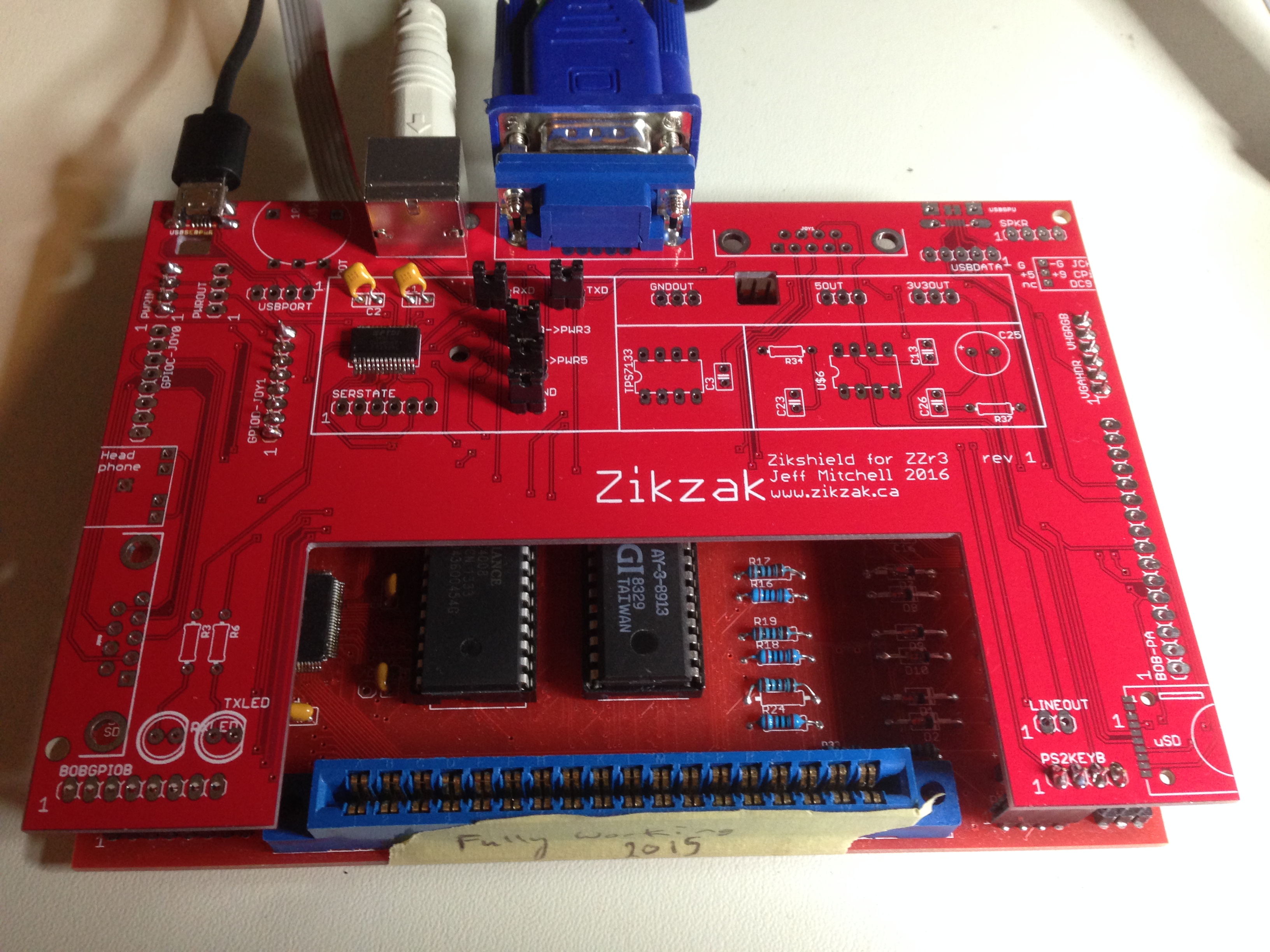
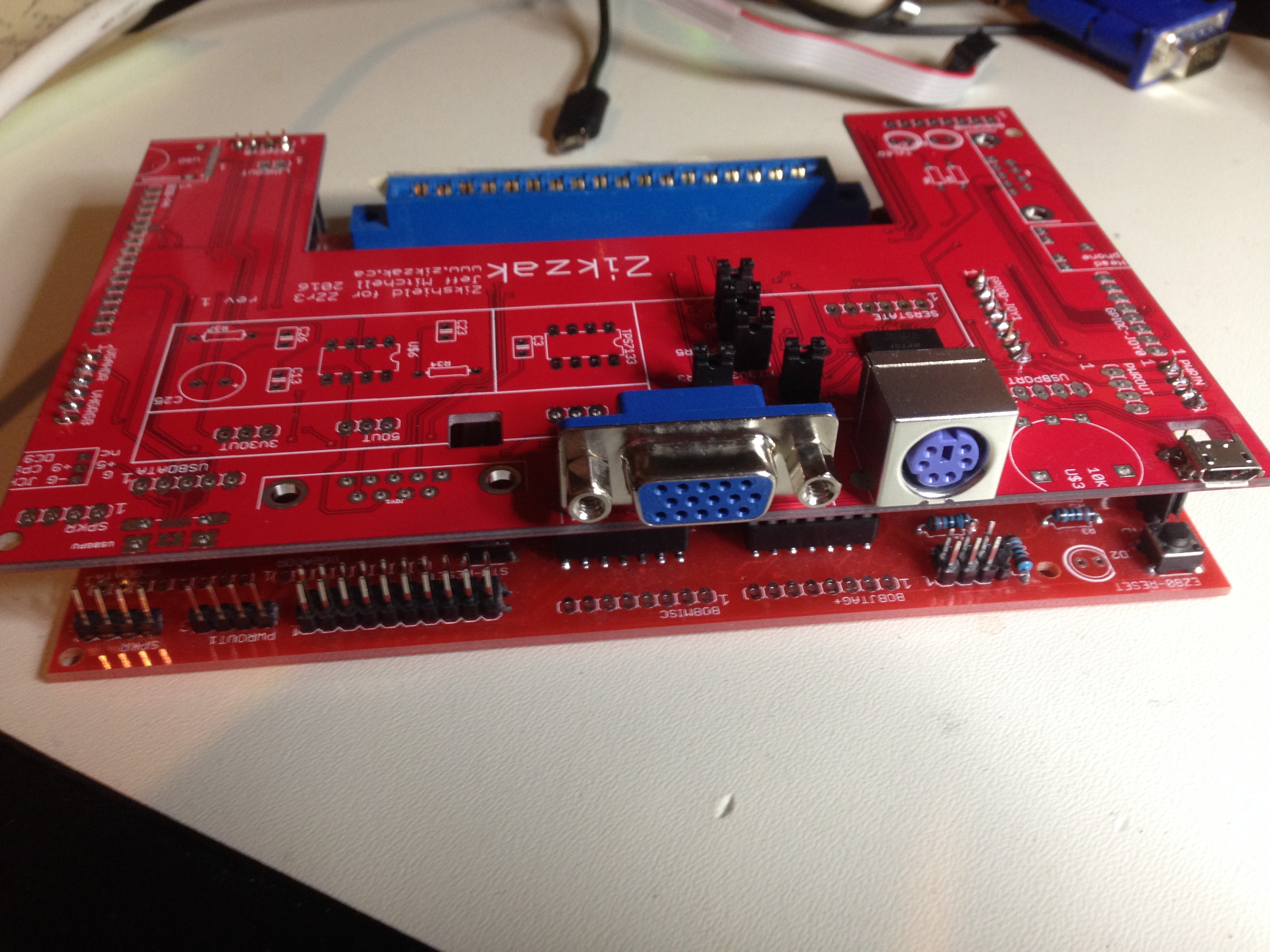
I'll probably end up making an r4 "all in one pcb" or maybe two board as above, anyway, of course, since its all fun But for now, r3 (already have it, and got one working a treat!), so just put together a $50-for-10 shield, populate one, and see how it goes!
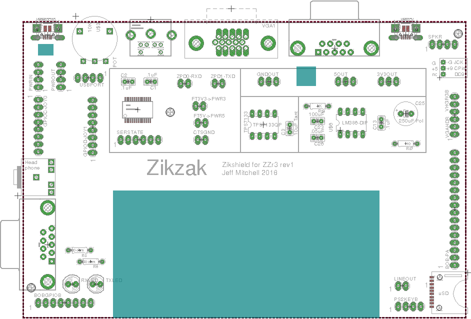
As you can see above, its already half done, and the hard part is out of the way; I know how I'm going to power it, and the power+usb+amp+ftdi circuit is already actually all schematiced up; the jacks and such are modeled and all on the schem and pcb; I need to worry over placement, and route all the unrouted traces .. but routing on that is a cakewalk! Routing could take a night or two only and done.
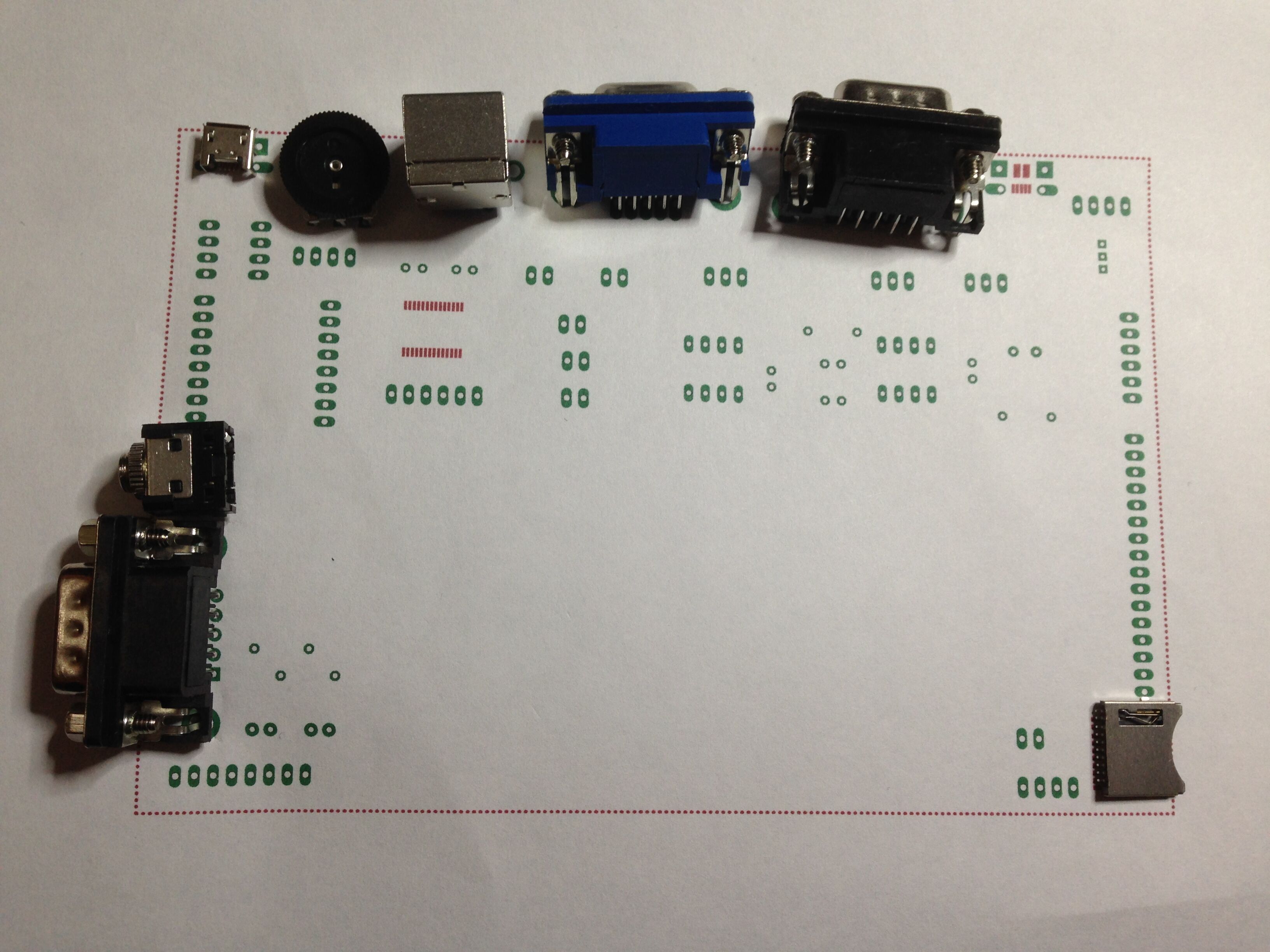
So, plowing ahead ... but not too fast, don't really want to screw up; need to check, re-check, re-re-check check the design rules, make sure nothing is too close; print out on printer, plug jacks and such through paper, amke sure things all fit and the physical real world casings and such don't get in the way in unpredicted fashion. Make sure it qll lines up between layers, and that the things fit vertically with no bits too tall for the header pins I'm meaning to try to use. I'm not using real board to board interconnects.. just really tall header pins, so need to measure it all out.
Still lots to do, but I enjoy it, for some reason
[doublepost=1463197753,1463195625][/doublepost]Redid the top edge (not cart side, the other one) milling; since that big block was really just to ensure theres space for te ZDI and JTAG .. rather than block out the whole top edge, just mill out right over those two spots. (Theres more header pins there, BOBJTAG+ and BOBMISC, but I don't really plan on using any of those pins; and if I do, could just run jumpers from the ZZr3 base pcb anyway. So, if I leave most of that top edge present, milling out just over the ZDI and JTAG headers themselves ad a bit more, it buys me back a bunch of edge space.. just enough to put JOY1 (second) and VGA between the ZDI and JTAG; I can get the PS/2 keyb connector on the back (top left, beside the power/serial USB) and then put the data USB on back (top right), which has the right symmetry to make me happy. The only wonky stuff then is the thumbwheel for volume, and the uSD, which are both sort of stranded in the middle-right, when they should be on the edge. Now mind you, they're still operable in the middle, which is fine; and uSD could even be left like that.. just stick an SD in there and not worry about it, right? But the thumbwheel I really would prefer to be exposed, so if I 3d print a case, it could be used
Anyway, need to relax a bit, will worry about this more over the weekend. Need to print it out on the ink printer, plop jacks into the paper, and see how it feels in the real world.
jeff
[doublepost=1463198818][/doublepost]and FWIW .. still adding subsets of the forum posts here, to the dev blog; you may want to also follow there:
http://zikzak.ca/dokuwiki/doku.php?id=devblog
The sweet spot for pcbs these days is still 4"-square or less (10cm and less to a side); so, I've often liked the idea of a stack of 2 4"-square boards. I've even gone so far as to do a buss up one side, so that 2 or 3 or 4 boards could sandwhich together like that.. a cpu board, a gpu board, a power/audio board, an expansion/cart board on top. Think of the madness! I went once to the extreme, wher eyou could even stack multiple cpu boards ... and even so far as a crazy bus, where you could put like 32 cpu boards together for some crazy fun....
The trick of course is that microcontrollers, with the pincounts I need (100+), are pretty 'big' (their footprint, plkus the necessary space around them for the routed paths), so putting two of them on the same 4" surface is hard. But as they're smt, there _is_ the possibility of doing one on each side, but I find I need those vias and both sides to do the horrid routing. This of course is why modern pcbs are 4+ layers thick, so you can jam things in good and route all around no problem.
So, hence why I've settled on 6"x4" .. a little pricier, but at least its got the space to put the two chips on there, and also enough for a bunch of support stuff.
But yes, I could do a r4 with various combinations..
- a base 6"x4" board with most of the good stuff
- a shield that goes on, for all the jacks and breakout
--> but designed for this purpose
ie: group all the headers together in some central location, or convenient location (elevator shaft like).
Making r3 was _Really_ tough routing, because its a metric hellpile of traces; also, the chip pinouts are really bizarre.. like, you'd think they'd be in bamks of 8, like on 8bit chips like the atmel avrs .. so GPIO "bank A" would be A0-A7, right? But on these high pincount chips, they're will nilly, 100 or 144 pins all in a big random mess more or less. Seems to me like they lay out the internal mess and when they add the physical pins on, its 'best they can do, without much of a fight/cost'; real boards are BGA surface mount and auto-routed by million dollar software so who cares right? But us hobbyists agonizing ove cost and every trace, it hurts like hell
And as noted, making the eagle cad library for these little jacks and parts is fiddly work; so making this shield for r3 is really just a way to move forward 'path of least resistance'; its easy to make the shield, and forces me to get the library drawn up; then I can get it made, and see if the library stuff is actually all right, the holes are in the right palce and measured right, and the pads connect to the right pins on the schematic, and the schematic circuits are all right, and etc etc; if the shield actually works (or has minor flaws easily corrected, or iterate a few revisions to get it right..), then you prove all that stuff.
After that, then if we still want a r4, we can plan that out and attack that, with having all the foundations again proved. Step by step, less risk; more time, but easier bites to make.
I'm one of those bloodyminded determined people, put one step in front of the next to get through the storm; real life makes no free time, but I'll be damed if I dont' make some progress any way I can. So this is what works for me
I'll probably end up making an r4 "all in one pcb" or maybe two board as above, anyway, of course, since its all fun
As you can see above, its already half done, and the hard part is out of the way; I know how I'm going to power it, and the power+usb+amp+ftdi circuit is already actually all schematiced up; the jacks and such are modeled and all on the schem and pcb; I need to worry over placement, and route all the unrouted traces .. but routing on that is a cakewalk! Routing could take a night or two only and done.
So, plowing ahead ... but not too fast, don't really want to screw up; need to check, re-check, re-re-check
Still lots to do, but I enjoy it, for some reason
[doublepost=1463197753,1463195625][/doublepost]Redid the top edge (not cart side, the other one) milling; since that big block was really just to ensure theres space for te ZDI and JTAG .. rather than block out the whole top edge, just mill out right over those two spots. (Theres more header pins there, BOBJTAG+ and BOBMISC, but I don't really plan on using any of those pins; and if I do, could just run jumpers from the ZZr3 base pcb anyway. So, if I leave most of that top edge present, milling out just over the ZDI and JTAG headers themselves ad a bit more, it buys me back a bunch of edge space.. just enough to put JOY1 (second) and VGA between the ZDI and JTAG; I can get the PS/2 keyb connector on the back (top left, beside the power/serial USB) and then put the data USB on back (top right), which has the right symmetry to make me happy. The only wonky stuff then is the thumbwheel for volume, and the uSD, which are both sort of stranded in the middle-right, when they should be on the edge. Now mind you, they're still operable in the middle, which is fine; and uSD could even be left like that.. just stick an SD in there and not worry about it, right? But the thumbwheel I really would prefer to be exposed, so if I 3d print a case, it could be used
Anyway, need to relax a bit, will worry about this more over the weekend. Need to print it out on the ink printer, plop jacks into the paper, and see how it feels in the real world.
jeff
[doublepost=1463198818][/doublepost]and FWIW .. still adding subsets of the forum posts here, to the dev blog; you may want to also follow there:
http://zikzak.ca/dokuwiki/doku.php?id=devblog


