Newbie at PCBs development


Xcl4m4t10n

Advanced Member
Joined
Dec 18, 2009
Messages
1,209
Hello community!

I NEED to develop some simple PCBs for a project I am running. The idea is to make a 1 layer PCB with a very simple production: It only have to send a sign from point A to point B. The problem is that I have no idea about PCB development so I have few questions to start:

- What software do you recommend for simple use/user?
- Must I have some considerations while I develop it.
- I want some "holes" on the board (i need to plug buttons there). The development software can do it or must I use another software?

This is the first questions, thank you in advance!
 
For a very simple projects, even only with THT (through-hole technology) components, KiCAD is usually OK. The advantage of it is that it's free.
Generally there are many tutorials for KiCAD, but the workflow is:
1. You design a schematic.
2. After verifying the schematic you end by adding power flags (information that program should transparently connect all Vcc and GND lines) and marking non-connected pins as not connected. Make sure you mark all of them! If you miss a pin and pass such schematic to next steps, it may be accidentally brought to e.g. ground. Generate component numbers and go through DRC test.
3. Generate the netlist from schematic. The netlist is an information what component's which pin links where, without any info about location or wire cosmetics. This is used to transfer schematic to PCB.
4. Fetch the netlist into CvPcb, assign packages to all components. Save.
5. Re-generate the netlist in Eeschema then! Even if it crashes you have a previously generated netlist, now it doesn't crash as it was crashing a few years ago.
6. Open CvPcb and fetch netlist with packages there. Spread the components and observe the "ratsnest" (straight lines) connections. By default you see from top. ARE ALL PACKAGES OK? Haven't you e.g. flipped a transistor? Make sure about it!
7. Draw outline of PCB.
8. Before placing and connecting components, edit design rules and set e.g. minimum track width used by factory. If you use the cheapest "cloth iron" method the 25-35 will be a bit thick but very easy to make. 1mm is ca. 40.
9. Start components placing by things you have to put in specific places. Connectors, LEDs, controls, mount holes. Then place other components to minimize ratsnest connections crossing over. Then design tracks.
10. The next day you'll find the way to connect it even better :).
11. Generate fill areas if you need. In DIY they can save lots of chemicals. You design them, configure, then commit by performing DRC check of board design.
12. For DIY, print on a normal paper to verify scale. For manufacturing, Gerber format is usually accepted by plants.

For more advanced projects, there are many commercial tools. The most sophisticated is Proteus (with simple simulator), in which the whole package/netlist process is automated but if you have something in specific package it requires fiddling.
 
KiCAD has a lot to be said for it, but I wouldn't say it's especially easy to use.
If you're likely to be doing more PCB design work in future, it's probably worth the effort to learn, but other tools do exist.

Fritzing, for example, is another FOSS tool that is much easier to get started with. It isn't a professional tool by any stretch of the imagination, but it does mostly work...
 
Thank you both for the information. As I said, the idea is just a very simple board for now, so I'm going to try these tools in 2 or 3 days and see what's happen. Hope you can help me with questions!
 
I struggled with KiCAD, but I managed to build a few boards using DesignSpark, then getting them manufactured at OSHPark.
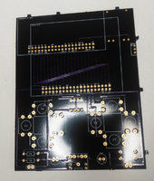
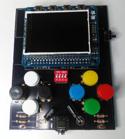
Here's my latest endevour
 

Attachments

  • IMG_20171211_093345.jpg
    IMG_20171211_093345.jpg
    94.9 KB · Views: 136
  • IMG_20171211_093354.jpg
    IMG_20171211_093354.jpg
    87 KB · Views: 132
I would not recommend Fritzing for a project. The biggest problem is that it gives too much ambiguity in design. The board is shown in a top view. Half of components in library are shown in top view. The second half is shown in something like front view, but not entirely. It's then impossible to see what is behind them. Want to put decoupling capacitors behind voltage regulator? Forget, they won't be seen in a design. The equivalent for visualizations I use is DIYLC, but this tool is in Java, You have been warned :).
I started with Protel, but I never made any PCB in it. Then I tried quite older version of Proteus and finally settled on KiCAD. However, I don't use SMD technology.
 
Fritzing, for example, is another FOSS tool that is much easier to get started with. It isn't a professional tool by any stretch of the imagination, but it does mostly work...

runs on debian too. its ok for simple boards a little bit of a learning curve. i managed to design a LM386 amp board on an Acer netbook running debian jessie.
 
Just to make sure: Do you need to design the pcb?
If not you can always buy a solder board, it already has large holes in it, somewhat the same experience as a breadboard.

If you need to design the pcb you could try Eagle.
 
Back
Top