Break out Bord for EXT (PCB Designer Needed)

Would you buy a TinyBoB


  • Total voters
    56

Nardella

Member
Joined
Mar 4, 2011
Messages
352
[Edit]


We want to improve the design before production, your input is requested.


Peca is considering having a PCB manufactured that he is calling TinyBoB, this is to make it easier to solder to the EXT connectors available from WizardStan.


The PCB will be 1.2mm thick or less and may look something like the attached image.


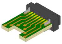
I have made a sketchup file of what it will look like when it is ready to be soldered to the EXT connector you can see a rendering of it attached, I intend to release the file once it is polished with peca's permission (peca I need will pm you with some questions about the PCB dimensions tomorrow).


I have some questions and suggestions:


1. I suspect that it might be a good idea to shorten the traces so they end something like .5-.75mm away from the edge to prevent any problems with solder going from one side of the PCB to the other side. What do you guys think?


2. I have never soldered wires to pads before, I trust it is not to difficult to learn to do?


3. How strong are pad connections compared to through hole connections?


4. It should be possible to modify the PCB design to have holes instead of pads, but would this increase cost?


5. What is the purpose of the cutout in the PCB, would removing this change the cost?


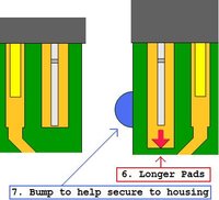
6. I think it might be a good idea to increase the length of the pads that accommodate the metal clips to enhance strength.


7. The pads on the outermost pins go straight to the edge, could this cause problems?


8. Would it be a good idea to have the PCB include physical features to facilitate securing it in some kind of casing, maybe solder pads too?


Thanks so much peca WizardStan and others who are working on EXT port projects. I hope you guys can help me with my media control project.
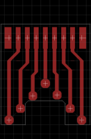
tinybob.png

EXT With tinybob.png
 
Last edited by a moderator:
Hi. Actually, I'm pretty lame in designing PCB. So this is only my idea and other guy designing it in Eagle. But he has no practice and low experience in overall - he studying and knowing how to use Eagle which I'm not used to use.


To clarify some question from my point of view:


1/ Yes, I intend to leave 0.5 mm blank edge.


2/ Just put little drop Sn on pad, little drop Sn on wire and then solder together. Some soldering resin or paste could be handy.


3/ It is not good to pulling wires off. I'll thing that appropriate shrink insulator should help or gluing or bonding cable with PCB nad/or housing... I'm think that applying force on wires is not good idea.


4/ Yes, drilling could costs more. It should be better to have drilled PCB and it not costs too much more.


5/ Cutout is intended for cable - for cables better positioning. And yes it could costs more. I didn't think on this so I didn't ask for cost of cutout. Maybe it couldn't be cutout, just space that could be filed out.


6/ I'm not get it. Do You mean those little metal plates on sides of connectors? If yes then yes :) It was intended to be soldered to short pads in the front corners of the PCB.


7/ Don't know, but plane is to have little empty space on the edge. However this is not clear from my simple draft.


8/ I'll use plastic housing from USB A connector. Loot at attachment: usba-housing.jpg
 
Last edited by a moderator:
3. I guess strength shouldn't be too much of an issue. I bet we could enhance strength if we solder useless wires to the little metal plates on the sides of the connectors, but the work is already very hard.


4. I imagine that drilling will cause problems with cost and quality, I suspect investigating holes is not worth our time.


5. Okay, thats what I thought it might be for, should probably keep it even if there is some cost.


6. Yes that is what I was talking about, I was suggesting making those pads bigger look at the attachment.


7. I was thinking something big, so that i could be filed to fit in various housings, see my attachment.


8. Do you have a specific part number in mind?

EXT With tinybob enhanced.jpg
 
Last edited by a moderator:
4/ I'll ask manufacturer. I think that it is manufactured by some kind CNC anyway, so shouldn't be an issue. If it not costs too much it it worth.


6/ OK, I'll just don't check it with connector drawing exactly.


7/ I see. I this case I'll rather let Cu cover PCB on the very edge. In various housing it could be used as securing it on place. Could be filed out if needed.


8/ No. It's random catch in local store (maybe I have to buy hundred of them before sold out - but I waiting for connectors to assure that it fits) :-/ I can't find it on the internet. Internal space is 11 x 4 (front profile) x 15 (longness) mm.


I'm attaching Eagle project with tinyBoB from one guy. Fell free to modify :)


---


EDIT:

I definitely think that trough hole PCB will be better, but could it be done in such small form PCB? But yes, if You are willing then I gladly accept You help B-)
I actually think that maybe through hole is not he best way to go, doing this would mean enlarging the PCB significantly and I suspect it may even be HARDER to slolder but I cannot say for certain. (I practiced a bit of soldering to the pads on a 32MB stick of ram).
OK, so let's go without holes.


---


EDIT2:


I checked price for drilling. It is the same as I think it is for non-drilled PCB. Actually non-drilled PCB is cheaper about $0,17 per square dm. Anyway, I have to call manufacturer to ask details. This PCB is really tiny and this shape...

tinyBoB.zip
 

Attachments

  • tinyBoB.zip
    23.4 KB · Views: 428
Last edited by a moderator:
I'm attaching Eagle project with tinyBoB from one guy. Fell free to modify :)
I can't figure out how to load that project into eagle. Tried putting in in the projects folder in the Program Files folder but no luck.


Figured it out.
 
Last edited by a moderator:
I'm attaching Eagle project with tinyBoB from one guy. Fell free to modify :)
I can't figure out how to load that project into eagle. Tried putting in in the projects folder in the Program Files folder but no luck.
Weird, I unpack this into "eagle" folder in my documents (win 7) and open it in Eagle flawlessly. I'll download free Eagle version 5.11. PCB seems to be designed in Eagle, version 5.08


EDIT: I try to learn some minimum in Eagle, as I have basic PCB design, maybe I manage to shape it.
 
Last edited by a moderator:
through hole soldering would be easier for the "novice" than pad soldering.


Idk how much extra that would cost
 
The pads will tear off if people try hanging wires off of them without epoxy or an enclosure to support the wires. Development stuff usually gets tossed around on the desk and one wrong move will destroy this thing. It's a definite advantage of through holes.
 
The pads will tear off if people try hanging wires off of them without epoxy or an enclosure to support the wires. Development stuff usually gets tossed around on the desk and one wrong move will destroy this thing. It's a definite advantage of through holes.
I spent time practising soldering to pads on sticks of ram, the connections are surprisingly strong.


After my experimentation I determined that pad soldering is not much harder than through hole and connections were sill quite strong.


Through hole will take up much more space meaning larger connectors. Also through hole may be trickier than pad.


Two part epoxy that would work well can be purchased at a dollar store. I believe that even if we go with through hole this would still be a good idea,
 
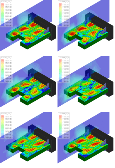
See attached gif.
Thats really cool looking tho I do not know what it means. Did you happen to use my models?
It is the electric field distribution when exciting two of the traces. I used your Eagle model, generated a Gerber, converted into HFSS and then created the remaining 3D solids.


I think the idea of connecting this PCB to the connector would help many people on soldering the TV cables.


Thanks for your ideas and please keep working in this project. Many users will be very glad to play their Pandoras on the big screen.
The Eagle model is not my work, it was uploaded by peca, I think a friend of his created it. I created the Sketchup version.


Also, what can we use the information about the electric field distribution for?
 
Also, what can we use the information about the electric field distribution for?
Well, in a HFSS electromagnetic analysis I can actually get S parameter data, in other words, this can give me attenuation on the traces (not the case here because they are very short) and electromagnetic interference between the traces (we call this crosstalk - not the case here because the frequency of the signals are relativelly low I believe). The electric field plots can tell me if this product will pass FCC or CE specifications, for example. I can also get temperature on the traces due to Joule heating (even though this is not the case here I´m sure because we have very low currents). This is a very simple PCB (even though very clever with a very good purpose).I just made this for fun and wanted to make it look cool :)
 
I try Eagle and I guess that posted design is without bottom side. I thing that guy only draw what I suggest him without thinking about other instructions in email :-/


I'm just sitting in work and catching release date, so no time to messing with CAD SW which I don't how to use it. So, if there is anybody willing redesign it in proper form, it will be very nice...
 
whats the ext connector under in the parts in eagle?


Not used to eagle only used multisim but there isn't a mac version of it :(
 
Last edited by a moderator:
Juliano: nice work! You are obviously in this field professionally, or .. student?
 
I try Eagle and I guess that posted design is without bottom side. I thing that guy only draw what I suggest him without thinking about other instructions in email :-/


I'm just sitting in work and catching release date, so no time to messing with CAD SW which I don't how to use it. So, if there is anybody willing redesign it in proper form, it will be very nice...
OK, I'm little stuck with this, but I'm decided to get into Eagle. Shame on me, neither today nor tomorrow. I'll hope for Thursday nigh.


So, any help with this staying appreciated.


---


EDIT: It is not must be in Eagle. Any PCB designing SW that is free for hobby use and gives gerber output is good enough. More simple to use and learn = better for me :) Eagle is just one that I heard about and is free for hobbyist.
 
Last edited by a moderator:
OK, I'm little stuck with this, but I'm decided to get into Eagle. Shame on me, neither today nor tomorrow. I'll hope for Thursday nigh.


So, any help with this staying appreciated.


---


EDIT: It is not must be in Eagle. Any PCB designing SW that is free for hobby use and gives gerber output is good enough. More simple to use and learn = better for me :) Eagle is just one that I heard about and is free for hobbyist.

Try design spark. Much easier and more intuitive to use than Eagle, and completely free (as in beer). Eagle really is kind of archaic and a real pain to use (IMHO), the problem being that almost every manufacturer still releases their part layouts for eagle only. The good news is that design spark is compatible with all eagle file types :D
 
I'm going to try and make a right angle breakout board file, I expect that this may be better for lots of things, what do you guys think?
 
Back
Top