Replacing My Nand With 1gb


nubie

Recovering Jerk-A-Holic
Joined
Oct 19, 2005
Messages
2,749
Location
USA California
Website
Visit site
I have a GP2X that is bricked, I have run the Jtag program multiple times, and I even ran a program to blank the NAND, and the result is always the same, a complete stop when uboot tries to probe the NAND.

I have a lousy MP3 player that I broke nearly as soon as I bought it, so I pulled it apart and found it was using the same pinout of the chip in the GP2X:

Full size download
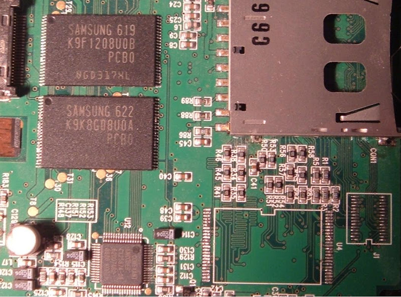
gignand.JPG


The one above is the original, the one below is its replacement.

I am stuck here because I have no flux or solder wick. I really need to clean up the pads, the solder is so high it is impossible to line the chip up. Also when I de-soldered the 1GB chip I wiped a lot of solder into the pins and that needs a clean up.

Does anyone know what will happen if I do this? I presume that it should just work, as the protocol and pinouts should be the same. (if the NAND chip is still good. if this doesn't work I guess it is OK, I had two busted units, and I would still have the same.)
 
I assume you have SMT soldering tools? This will be one hell of a soldering job if you do not.

I would assume it would recognize it, but I do not know if it will see it as 1gb.

If you are able to pull this off, I think you should make one with a 4gb nand. That would sell for quite a bit on ebay, especially because it bypasses the uber-slow SD write speed on the GP2X. :)
 
palmertech said:
I assume you have SMT soldering tools? This will be one hell of a soldering job if you do not.

I would assume it would recognize it, but I do not know if it will see it as 1gb.
Nope, just a 30watt and a 15watt iron from radio shack. If you check the pinout 1-6, 10, 11, 14, 15, 20-28, 33-35, 38-40, and 45-48 aren't connected, so I suppose I could bridge them together or to one neighbor without a problem. That is only 19 out of 48 pins that need to be connected properly.

It shouldn't be too difficult, I think I am going to employ the wipe a ton of solder onto it and then use solder wick to suck most of it back off method.

This is an awesome video btw (what I wouldn't give for his stereo microscope :)): http://www.youtube.com/watch?v=3NN7UGWYmBY
 
Last edited by a moderator:
palmertech said:
If you are able to pull this off, I think you should make one with a 4gb nand. That would sell for quite a bit on ebay, especially because it bypasses the uber-slow SD write speed on the GP2X. :)
Interesting, I wonder what the chips cost? Might be worth it. If only there was a Dpad mod that didn't involve tearing up a lot of controllers or GB handhelds.

I don't know how much faster this is than the SD, but it could definitely solve some storage problems, and you could even use it to load stuff onto people's SD cards :).

I wonder what the best method is to make the extra space accessible. Maybe just add another partition to the extra ~900MB of space and then mount it on the EXT? Or the NAND? Won't be needing that piddling storage area any longer :).

If anyone is knowledgeable enough with the GP2X and Linux to help me with that I would much appreciate it.

I will likely be going to the store and picking up some flux and de-soldering wick/braid sometime next week.

I just realized that I could put all my faves on the NAND, forget the SD entirely :), too sweet.
 
Last edited by a moderator:
Peter R said:
Your best bet is asking Orkie when he's awake tomorrow.
I guess, I think I upset him a bit bitching at the Wiz :unsure:

It is OK for me to wait a bit, I don't even know if this will work, and I won't know until I get the flux and solder wick.
 
Last edited by a moderator:
Peter R said:
I have a feeling that this won't work for some reason or another but it certainly would be very cool if it did.
I keep trying to come up with a reason it won't work, and frankly I just don't know enough.

According to the datasheets the pinouts are the same, the only thing that could be different is the capacity and model number, and why would it care what size or model the chip is as long as it can read and write to the address it wants to.
 
Last edited by a moderator:
Peter R said:
Maybe its hardcoded to only see 64MB ;)
Well, the linux libraries to read the NAND should be able to see it once it boots even if the Uboot can't, and I could put a separate partition (even a different file system) in the extra space.

Was Orkie DJWillis the guy making Open2X? I could switch to that and maybe it wouldn't be hard-coded where the original firmware is. I wouldn't mind open2x as long as I could use the binary blob that accelerates the mpeg4/divx playback.
 
Last edited by a moderator:
Just some food for thought:

4GB $10-12 http://search.digikey.com/scripts/DkSearch...e=557-1362-1-ND http://search.digikey.com/scripts/DkSearch...e=557-1363-1-ND

8GB $10-20 http://search.digikey.com/scripts/DkSearch...e=557-1414-1-ND

http://search.digikey.com/scripts/DkSearch...e=557-1373-1-ND

http://search.digikey.com/scripts/DkSearch...e=557-1371-1-ND

http://search.digikey.com/scripts/DkSearch...e=557-1372-1-ND

16GB $15.42 (I haven't checked the pinout on this, but it is an 8-bit parallel flash with 48 pins in a tsop that will take 3.3volts :) )

http://search.digikey.com/scripts/DkSearch...e=557-1374-1-ND

I find it funny that 4GB and 8GB are about the same price, and 16GB are nearly the same as well, does anyone know if there is a technical reason the 16GB chip wouldn't work, because if you could swap these out it would be a hell of an upgrade :).

I just checked the smaller capacity flash chips at digikey, the smallest they offer in a parallel 8-bit is 2GB for $7-8, it just isn't worth it with 16GB for $15 is it?
 
I'll paste what I put in your selling thread before I noticed this :p.

You *should* be OK with a 10us longer seek time, but remember that the kernel is hardcoded to the times for the old NAND, so you *may* get it marking blocks as bad if they take too long to respond. As for JTAG, it is meant to be connected to the CPU since it is actually for debugging most of the time, not flashing NAND chips.

And an addition.

Assuming it recognises the chip, there is no reason why Linux would fail to see the whole of the NAND because the final partition is always defined as MTDPART_SIZ_FULL (i.e. take up the whole of the space) in the MMSP2 NAND driver. I don't see why it would fail to recognise the chip, unless u-boot doesn't like it for some reason.
 
Just my 2 cents:
You should NOT bridge any pins, as they might stop the NAND from working.
You should also connect ALL pins to the board. The gp2x has a multilayer PCB. Some pins can actually connect via the inside of the PCB, and you can't see this with just your eyes.
 
Sorry to put a dampener on this but you really should be aware of this before you sink to much time into the project.

The MMSP2 SoC used in the GP2X can't use large block NAND to boot from the hardware bootloader only small block (i.e. low capacity older style NAND). The hardware bootloader is what will pull and run U-Boot from the NAND so if it can't see the NAND your sunk.

Large block V Small block NAND said:
]Large block devices ≥ 1Gb density.
[/LIST]
Small block NAND contain blocks made up of 32 pages, where each page contains 512 data bytes + 16 spare bytes (IIRC). Large block NAND contains blocks made up of 64 pages, each page containing 2,048 data bytes + 64 spare bytes. So for a 1Gb NAND device, this translates to 8,192 blocks in the small block organisation and 1,024 blocks in the large block organisation.
So you may well find this is going to be a depressing endeavour unless your happy to strap the boot from jTAG every time you power up and then use that to send over a modified bootloader to then launch something from your new NAND - For a handheld that is a little limiting ;).

There is one possible work around and that is using some large block NAND that supports Power-on Read Enable (PRE) mode to, in essence, emulate small page NAND when first powered. However I only recall Samsung ever made large page NAND with a PRE mode in volume and they EOL'ed all that that back in 2006 :(.

I have these supported chips that are large block with PRE mode support from an old MagicEyes note if you really want to try and track down a working chip.

Supported large block NAND with PRE mode said:
Capacity (Gbit) Part Number Maker
2 K9F2G08U0M SAMSUNG
4 K9K4G08U0M SAMSUNG
4 K9K4G08U1M SAMSUNG
8 K9W8G08U1M SAMSUNG
If you go for this then good luck but do not expect to just be able to pop a pin compatible large page NAND on the board and have it work. It is just not going to happen :(.

For reference the MagicEyes supported design option was to have a small page NAND chip for boot and a 2nd large page NAND for storage hooked up as a second NAND chip. Not going to happen on a GP2X ;).
 
Last edited by a moderator:
Orkie said:
You *should* be OK with a 10us longer seek time, but remember that the kernel is hardcoded to the times for the old NAND, so you *may* get it marking blocks as bad if they take too long to respond. As for JTAG, it is meant to be connected to the CPU since it is actually for debugging most of the time, not flashing NAND chips.
Thanks, that was maximum seek time, so it could be fine.

Orkie said:
Assuming it recognises the chip, there is no reason why Linux would fail to see the whole of the NAND because the final partition is always defined as MTDPART_SIZ_FULL (i.e. take up the whole of the space) in the MMSP2 NAND driver. I don't see why it would fail to recognise the chip, unless u-boot doesn't like it for some reason.

Interesting, that is good news.
EvilDragon said:
Just my 2 cents:
You should NOT bridge any pins, as they might stop the NAND from working.
You should also connect ALL pins to the board. The gp2x has a multilayer PCB. Some pins can actually connect via the inside of the PCB, and you can't see this with just your eyes.

Can they Via without a hole drilled? Because I can see a hole.

According to the datasheet I have there are unused pins, but I wasn't really planning on bridging solder. I want it to look and function as stock.
DJWillis said:
Sorry to put a dampener on this but you really should be aware of this before you sink to much time into the project.

The MMSP2 SoC used in the GP2X can't use large block NAND to boot from the hardware bootloader only small block (i.e. low capacity older style NAND). The hardware bootloader is what will pull and run U-Boot from the NAND so if it can't see the NAND you're sunk.

Large block V Small block NAND said:
]Large block devices ≥ 1Gb density.
[/LIST]
Small block NAND contain blocks made up of 32 pages, where each page contains 512 data bytes + 16 spare bytes (IIRC). Large block NAND contains blocks made up of 64 pages, each page containing 2,048 data bytes + 64 spare bytes. So for a 1Gb NAND device, this translates to 8,192 blocks in the small block organisation and 1,024 blocks in the large block organisation.
So you may well find this is going to be a depressing endeavour unless your happy to strap the boot from jTAG every time you power up and then use that to send over a modified bootloader to then launch something from your new NAND - For a handheld that is a little limiting ;).
Aagh, I knew there was a dumb reason that there weren't a lot of big nand mods :(. If I Jtag the unbricking uboot over and it can read large block NAND will it boot fine?

It would be a lousy work-around, but not too bad compared to no GP2X, at least I could play some games, or use it as a console to watch movies on :).

QUOTE
There is one possible work around and that is using some large block NAND that supports Power-on Read Enable (PRE) mode to, in essence, emulate small page NAND when first powered. However I only recall Samsung ever made large page NAND with a PRE mode in volume and they EOL'ed all that that back in 2006 :(.

I have these supported chips that are large block with PRE mode support from an old MagicEyes note if you really want to try and track down a working chip.

Supported large block NAND with PRE mode said:
Capacity (Gbit) Part Number Maker
2 K9F2G08U0M SAMSUNG
4 K9K4G08U0M SAMSUNG
4 K9K4G08U1M SAMSUNG
8 K9W8G08U1M SAMSUNG
If you go for this then good luck but do not expect to just be able to pop a pin compatible large page NAND on the board and have it work. It is just not going to happen :(.
For reference the MagicEyes supported design option was to have a small page NAND chip for boot and a 2nd large page NAND for storage hooked up as a second NAND chip. Not going to happen on a GP2X ;).

Thanks, I will peruse my documentation for the layout. Basically if I have 8,192 blocks I should be OK with my current chip? Regarding the PRE mode, how do I enable that if it is supported by my chip?

I guess it was a bit ambitious to expect onboard 16GB for $15, too bad really.

My goal is to get the darn thing booting with minimal cash outlay, I would use a 64mb (or whatever reasonably priced small block alternative is available), just to be able to use my GP again.
 
Last edited by a moderator:
I just checked the PDF, it is 2,048 blocks :angry:

I will check Digikey for a usable NAND now I guess, maybe I can order it with Uzebox components I want to get anyway :D .

Quick question if you guys know, what is the purpose of the unpopulated pad labeled J1?
 
HELP! HELP!

I want to buy a chip I know will work, but I can't find a place selling one, is there a list of flash chips the MMSP2 supports?

I can't find a samsung supplier. Would I be better off purchasing a 64MB mp3 player and stripping it of its NAND?

How about a pin-compatible 4MB chip, as long as the GP2X can boot on its own I can use a uboot that loads the kernel from the SD card.

Maybe I there is a compatible flash chip somewhere in my room, I have a WebTV and 3-4 Tivo motherboards here, I will check them.
 
DJWillis said:
Large block V Small block NAND said:
]Large block devices ≥ 1Gb density.
[/LIST]
Small block NAND contain blocks made up of 32 pages, where each page contains 512 data bytes + 16 spare bytes (IIRC). Large block NAND contains blocks made up of 64 pages, each page containing 2,048 data bytes + 64 spare bytes. So for a 1Gb NAND device, this translates to 8,192 blocks in the small block organisation and 1,024 blocks in the large block organisation.
I am searching for a good chip, but I am a bit confused.

1Gb as in 128 Mega Bytes?, or as in 1 GigaByte?
Here is a table I am working on to allow me to quickly find a compatible chip:
CODE

. . Number of Blocks
MB Mbit Good Bad

64 512Mbit 512 64
128 1Gbit 1,024 128
256 2Gbit 2,048 256
512 4Gbit 4,096 512
1gb 8Gbit 8,192 1,024


I don't think this looks right, and I can't look for a chip or price it until it does look right. (not to mention that Micron has put a NDA on Datasheets for **** ***** jerks.)

There is no stock of chips lower than 1GB and 64MB or larger right now :(,

If the Firmware would fit in 32MB there is this chip: http://search.digikey.com/scripts/DkSearch...D256W3A2BN6E-ND

Suggestions welcome (helpful suggestions.)
 
Last edited by a moderator:
I may have been overreacting a little (doesn't help that I seem to be on a different cycle, so communication takes a while)

This is the PDF for the chip that I plan to solder down, please let me know what you think:
http://pdf1.alldatasheet.co.kr/datasheet-p...K9K8G08U0A.html
QUOTE
512K Pages
(=8,192 Blocks)


QUOTE
1 Page = (2K + 64)Bytes
1 Block = (2K + 64)B x 64 Pages
= (128K + 4K) Bytes
1 Device = (2K+64)B x 64Pages x 8,192 Blocks
 
Back
Top